Digital I/O Signaling and Connections
Outputs
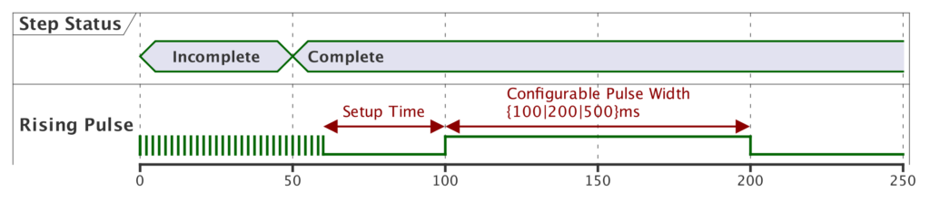
An output signal can be generated on any available output capable GPIO pin of the given IPC being used. Output signals are single pulses of a configurable pulse width.
There is a hard-coded 10ms setup time generated for every signal, so if multiple output signals happen to be back-to-back there is guaranteed to be at least 10ms of low signal state before the rising edge.
Inputs
Input signals used to start assemblies should look similar to the following timing diagram. Supercoach is looking for a rising edge.
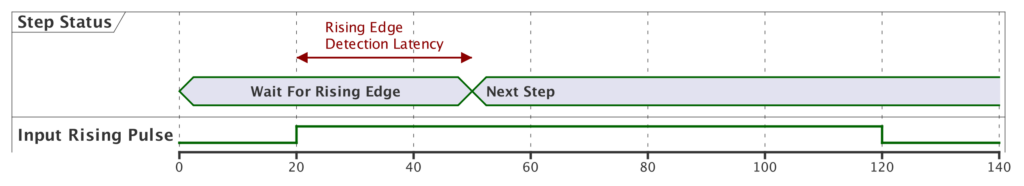
The input signal should be held high after the rising edge for at least 10ms. In the diagram above it is held high from 20ms to 120ms, or 100ms total, just as an illustration.
Hardware Specific Settings
Siemens IPC520a
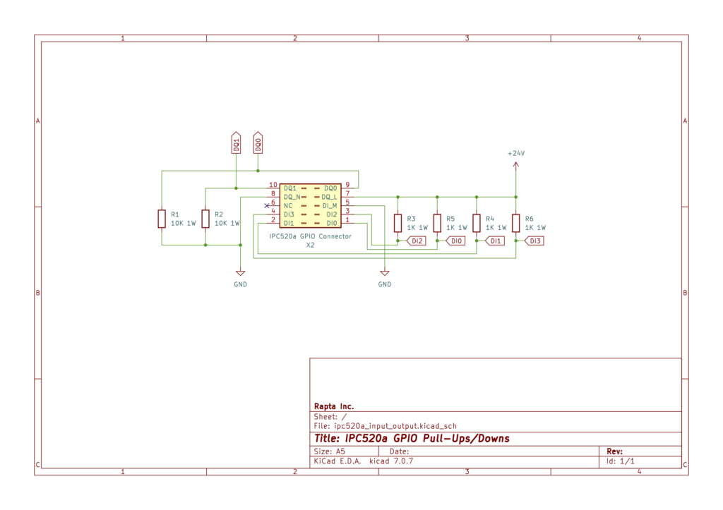
The following schematic shows the general biasing required for the GPIO signals to function correctly.
The important points shown in the schematic below are
DQ_Lmust be tied to+24VDQ_NandDI_Mmust be tied toGND- All
DQoutputs must be pulled down toGNDvia10K Ω1-Watt resistors - All
DIinputs must be pulled up to+24Vvia1K Ω1-Watt resistors
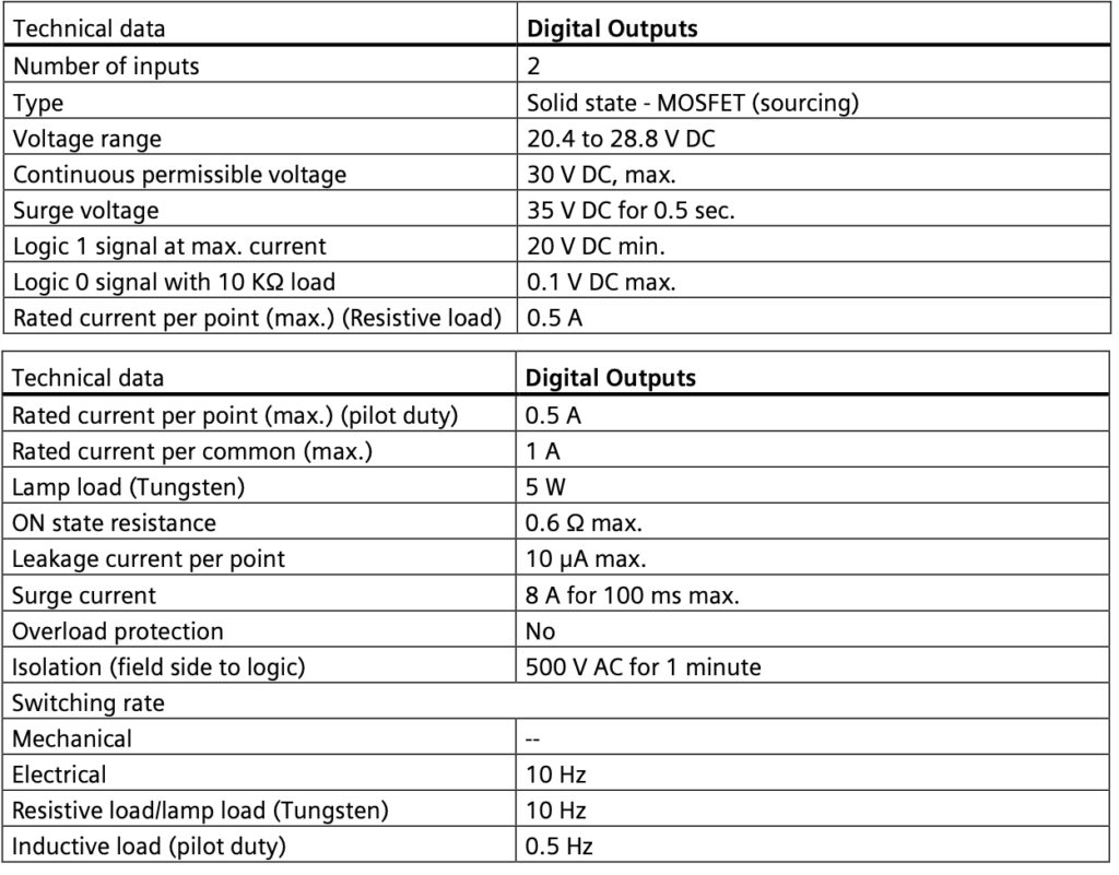
The following tables are taken directly from the instruction manual for the IPC520a and describe the voltages levels required to signify logical high/low signals.